
Solder Mask
What is Solder Mask?
 Solder Mask is a protective coating applied to the bare printed circuit board. Bare boards are covered with mask to prevent accidental solder bridging during assembly and to help protect the board from the environment. (Don't confuse solder mask with conformal coating. Conformal coating is also a protective coating but it's applied to the assembled board rather than the unpopulated bare board.)
Solder mask is usually green but many other colors are available. The most common colors we use are:
- Green
- Matte Green
- Red
- Blue
- Yellow
- White
- Black
- Matte Black
At PCB Universe, we use LPI (Liquid Photo Imageable) solder masks. LPI masks are by far the most common type of mask used today. They are more reliable, can be printed very accurately, and make better contact with the surface of the board and the copper features on which they're applied to protect. LPI masks are an epoxy based material so they are very durable and nearly impossible to remove once they have been cured.
In the past, masks were applied in sheets called Dry Film, but with the advent of Liquid Photo Imageable masks and techniques, Dry Film is rarely used today.
How is LPI Solder Mask Applied?
- The production panel is thoroughly cleaned to ensure no dust particles are trapped under the mask.
- The panels are completely covered on both sides with the liquid mask.
- The coated panels are placed in an oven to tack-dry the mask just enough to finish processing.
- A film is made of your solder mask Gerber files, one for each side of the board. Where you want mask to stick to the board, the film will be clear. Where the mask should be removed will be black on the film.
- The tack-dried boards are placed into a UV developer and the film is precisely aligned over the board. The blacked out locations on the film will prevent the UV light from curing the mask where it is not wanted.
- After the mask is exposed to the UV lamps, the uncured mask is washed off leaving mask only in the places needed.
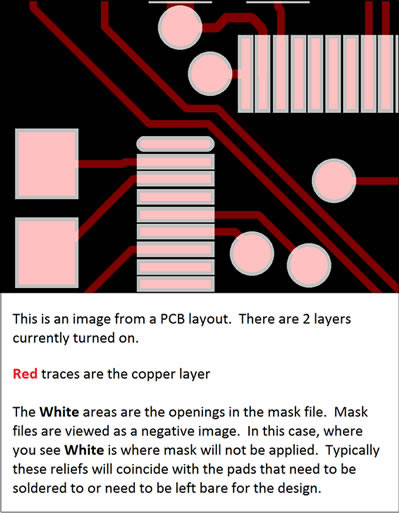
How is Solder Mask defined in my data?
 Solder Mask layers in your Gerber (CAD) data should be thought of as a negative image. This means where you see color on the mask layer is where you don't want mask coverage. Everywhere else will be covered with mask. Think of the solder mask as completely covering your board and your mask file shows the places where you don't want the mask applied.
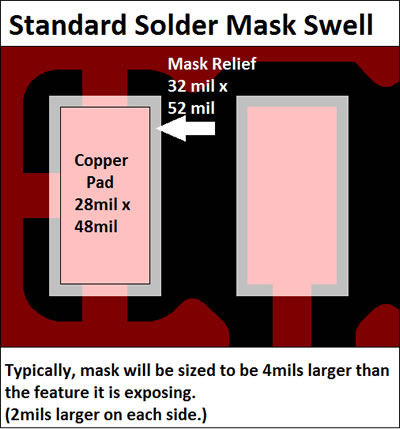
During the tooling process, we will automatically adjust your mask apertures as needed for production. Generally, a solder mask aperture will be adjusted so it is 4mils larger than the copper pad it is exposing (2mils larger per side). If we printed the mask exactly the same size as the copper pad, there is a good chance the mask would not be exactly centered on the pad which would result in some of your copper pad being covered with mask. The tolerance for mask placement is ±2mils so that is why we adjust mask apertures to be 2mils larger all the way around the copper feature helping to ensure the entire pad can be soldered.
There are times when a mask defined pad is required. A mask defined pad is when the mask relief is the same size or smaller than the copper pad it is exposing. These are generally used when mask dams are needed between SMD pads but there is not enough space to print a dam and follow the standard mask swell mentioned above. If you require a mask defined pad and do not wish your mask clearances to be modified, you must include a fab note stating which pads should not be adjusted.
Solder Mask and Assembly
Solder mask is very important when it comes to assembling your PCB. As any assembler will tell you, if it's possible, always put solder mask dams between your surface mount pads. This helps prevent accidental solder bridging during assembly and greatly reduces the amount of rework required to remove shorts.
Be aware there are limitations with regards to minimum pad to pad spacing so not all SMD (Surface Mount Device) pads will be able to have mask dams between them. Here are our minimum mask dam guidelines.
![]()
Solder Mask is also used to prevent solder starvation. Solder starvation can occur for many reasons but mask can prevent solder from wicking away from its intended location. Open vias near your surface mount pads (such as with BGAs), can wick solder away from the pad and down the open via resulting in intermittent or no connection. Mask is frequently used to tent or plug these vias to prevent this. A good rule of thumb to follow is, cover everything with solder mask unless you need to solder to it or use it as a test point. See our Tech Tip on Via Tenting, Plugging and Filling.
If you have any questions, please contact us; we will be glad to assist you with your array!